Cantilever Probes
Beryllium copper is a ductile, weldable and workable alloy, which can withstand non-oxidizing acids such as hydrochloric acid and carbonic acid. It is also resistant to plastic decomposition, wear resistance, and scratch resistance. In addition, beryllium copper can be improved by heat treatment. Strength and its toughness and conductivity.
Beryllium copper probes are also a cost-effective choice for applications where good conductivity and low pad damage are important.
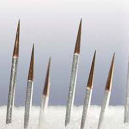
The outer tip of the beryllium copper probe is bright golden yellow, and the beryllium copper probe is the softest among all types of probes. Generally sold are electroless polishing, the probe is easy to oxidize and is not easy to clean, the original probe is electropolished, not easy to oxidize and easy to clean, and the impedance is stable.
Palladium alloy probe features:
Use new precious metal composite materials.
The LED wafer factory test is more suitable for spot testing of red and blue light, with high stability and long life.
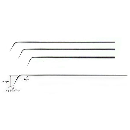
The needle tip is etched and polished, and the needle tip angle can be customized.
Taiwan's production quality is stable, the price is the most competitive, and it is specially developed and manufactured for the LED industry.
The probe is the main part of the probe card and is used for the connection between the electronic component and the tester so that the circuit board can be actually inspected for testing.
Use probe: It is the main component of the probe card and is used as a connection component. Separate tests can be performed by transmitting electrical signals to the chip pads to separate high-quality products from defective products.
Material: Tungsten (WNP), Rhenium Tungsten (WRNP), P4, P7, BC
Specifications are customized according to customer needs
Customized production can be made according to customer drawings and samples
Stable quality and fast delivery
Country of Origin: United States
Processing place: Taiwan
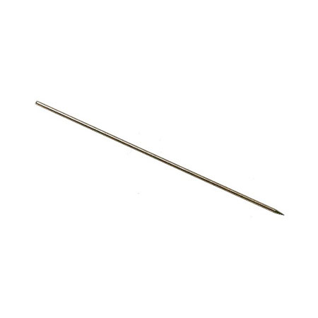
Tungsten needles can be divided into round rod-shaped tungsten needles and pointed tungsten needles according to their shape.
The rod-shaped tungsten needle has a slender structure and a metallic surface. Used for argon arc welding electrodes. Argon arc welding technology is the fastest growing and most widely used welding technology at home and abroad. In particular, manual argon tungsten arc welding has become an indispensable method for welding various metal structures.
During welding, an arc is generated between the tungsten electrode and the workpiece, and the filler metal is fed in from one side. Under the action of the arc heat, the filler metal and the workpiece melt together to form a weld. In order to prevent the melting and burning of the electrode, the welding current should not be too large. Therefore, tungsten argon arc welding is usually suitable for welding thin plates below 4mm, such as pipe butt joints, pipe and tube plate connection.
Tungsten needles with a pointed tip are mainly used for instrument probes, such as a digital four-probe tester, which is a multi-purpose comprehensive measurement device using the four-probe measurement principle.
This instrument is designed in accordance with the national standard of physical testing methods for single crystal silicon and with reference to the American A.S.T.M standard. It is a special instrument for testing the resistivity and sheet resistance (sheet resistance) of semiconductor materials.
Tungsten needles are mainly used in semiconductor material factories, semiconductor device factories, scientific research institutions, and universities to test the resistance performance of semiconductor materials.
 English
 Français
 Deutsch
 Русский
 Português
 Italiano
 हिन्दी
 Español
 Nederlandse
 العربية
 Tiếng Việt
 ภาษาไทย
 Bahasa Indonesia
 বাঙ্গালী
 Türk
Türk 繁體中文
繁體中文


